Here’s the overview of the I/O board that stands between the KIM-1 and the tiny terminals:
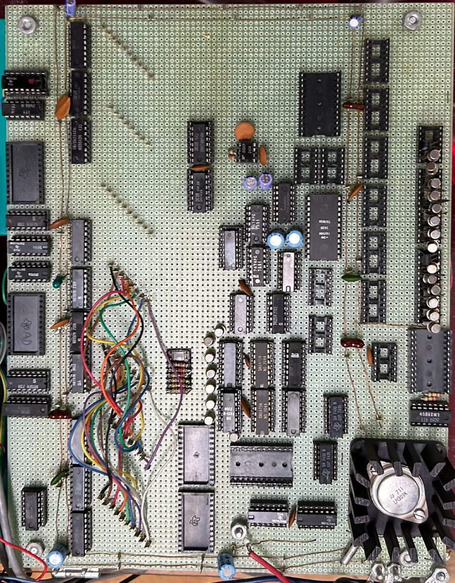
To show the components properly, I have removed the four ribbon cable connectors, two from the KIM-1 and two going out to the tiny terminals.
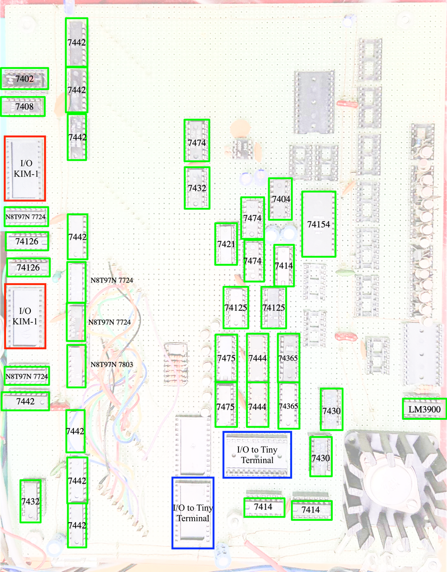
This shows the identities of the ICs and connectors:
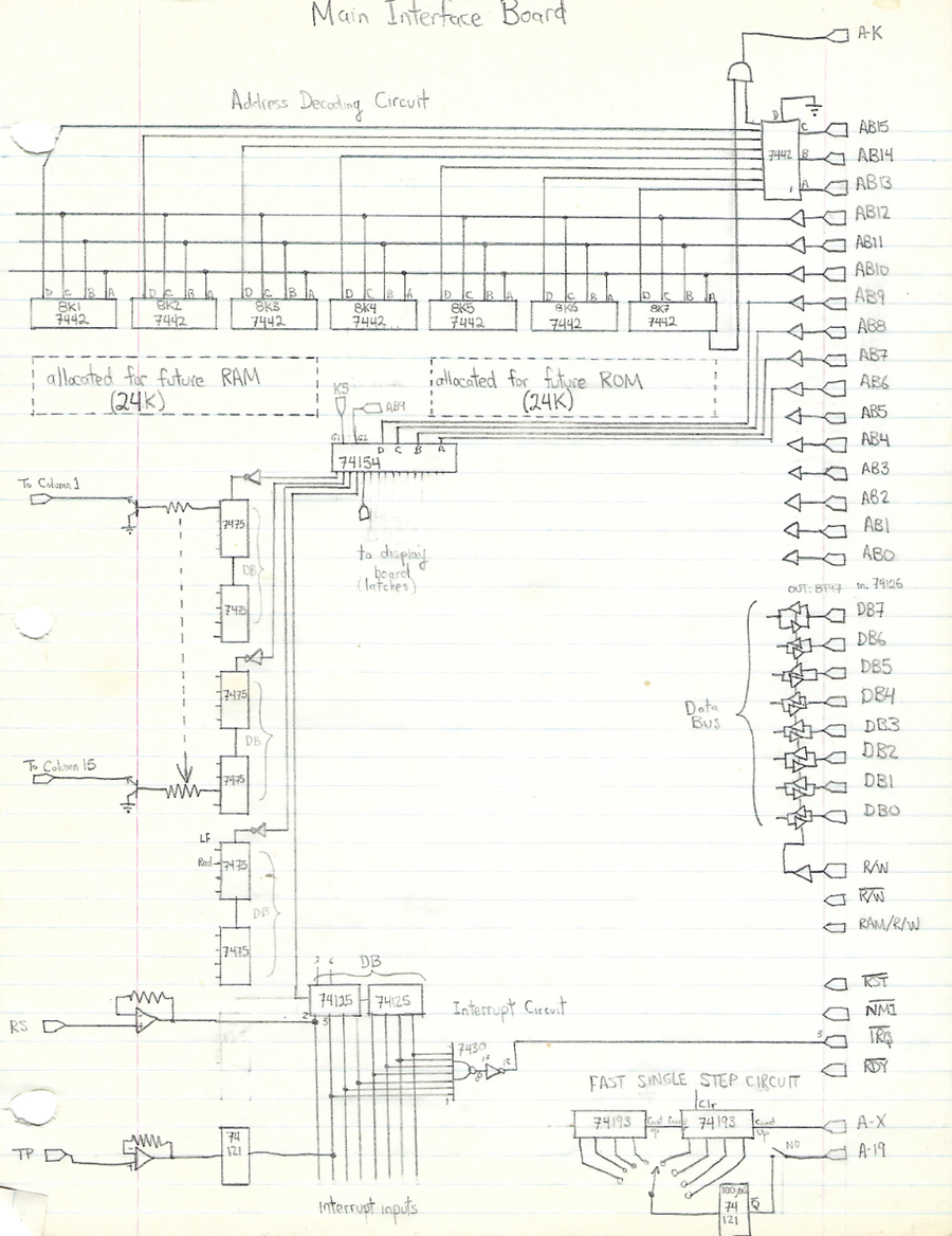
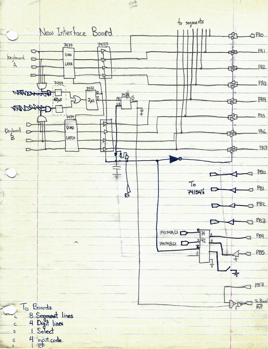
Here’s the circuit diagram from my records:
Here are short descriptions of the ICs on this board:
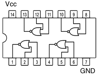
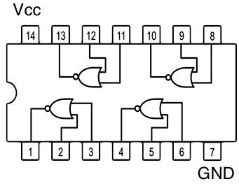
7402. Quad 2-input NOR gate
7404. Hex inverter
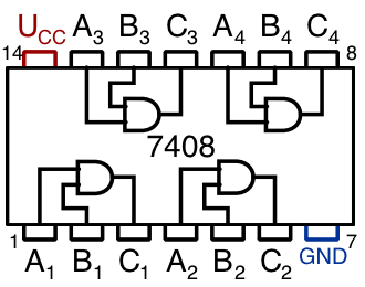
7408. Quad 2-input AND gate
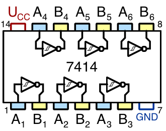
7414. Hex inverter Schmitt trigger
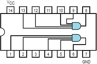
7421. Dual 4-input AND gate
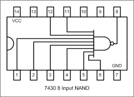
7430. 8-input NAND gate
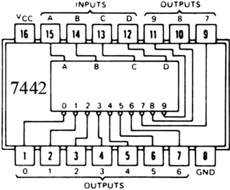
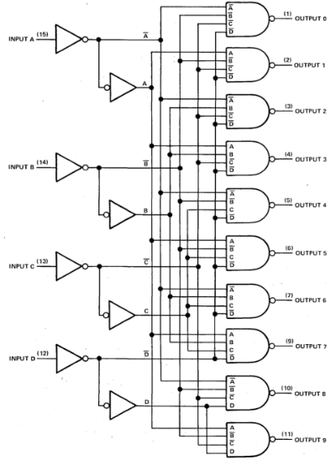
7442. BCD to decimal decoder
7444. 4−Line−to−10−Line Gray−to−Decimal Decoder
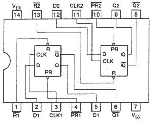
7474. Dual D flip-flop
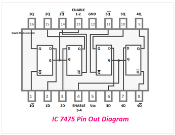
7475. 4−Bit Bistable Latch
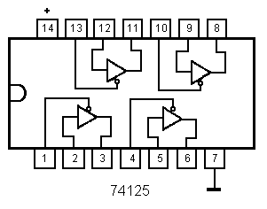
74125. Quad Bus Buffer with 3−State Outputs
74126. Quad 3-state Bus Buffer
74154. 4−Line−to−16−Line Decoder/Demultiplexer
74365. Hex bus drivers with 3-state outputs
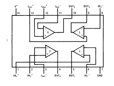
LM3900. Quad Op-ams
I intended to allow it to grow. That’s why there are so many empty sockets on the board. Here’s the backside of the board:
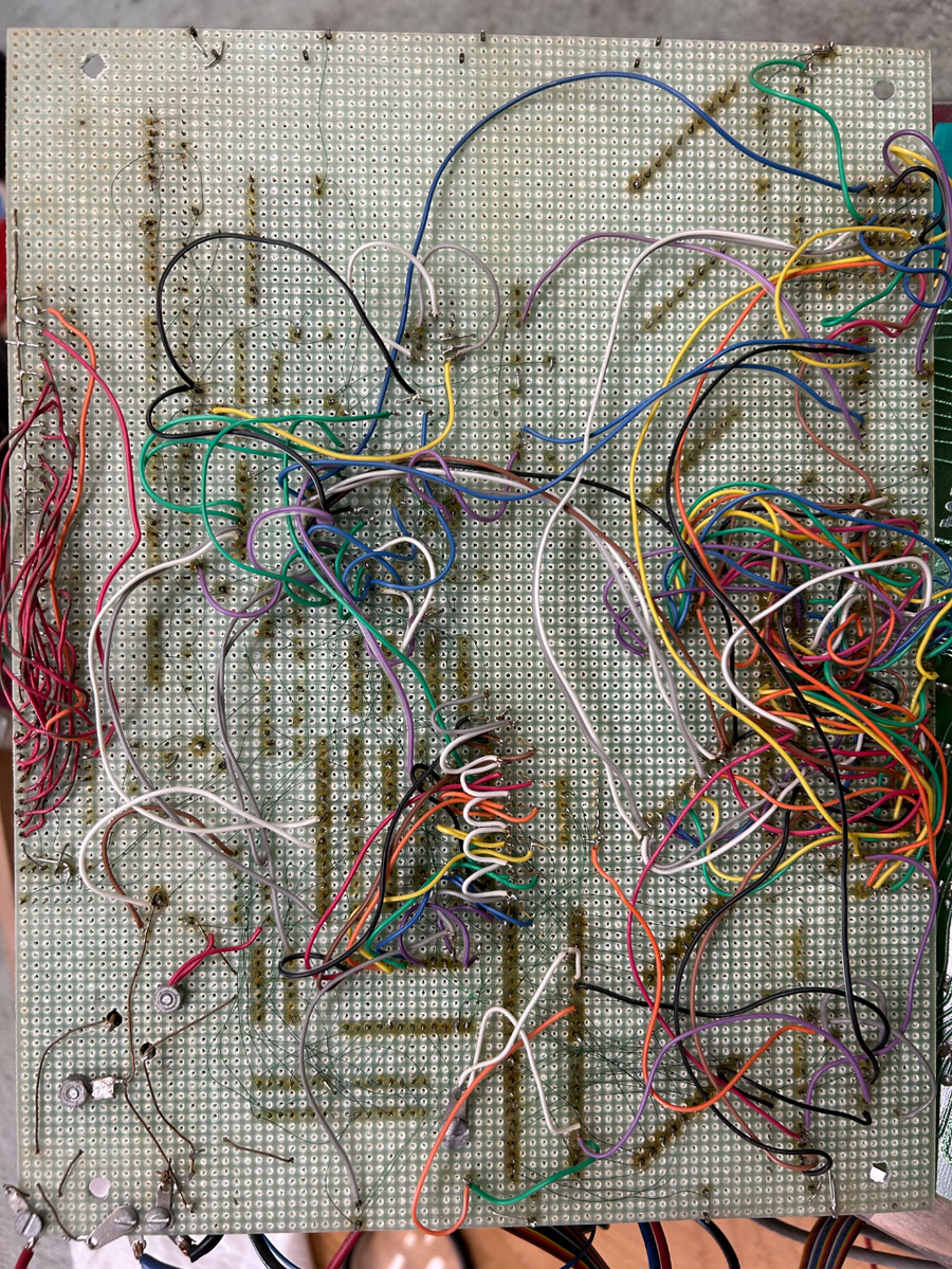
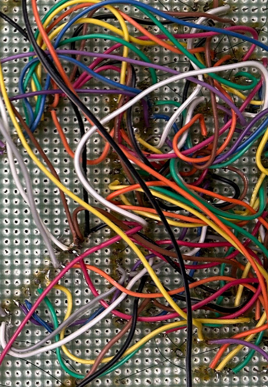
I have kept a higher-resolution copy (this is 1024h x 1365v, the big one is 3024h x 4032v) should anybody wish to trace the circuit, but I warn you again, tracing those wires will be all but impossible. Here’s a high-resolution image of just a small part of it:
Looks like fun, right? Well, I got lucky. Deep down in the storage boxes, I stumbled across a small binder full of details about my KIM-1 system, including a schematic. I don’t know how complete this schematic is; I’m sure that I made some changes along the way. But this should get you close: